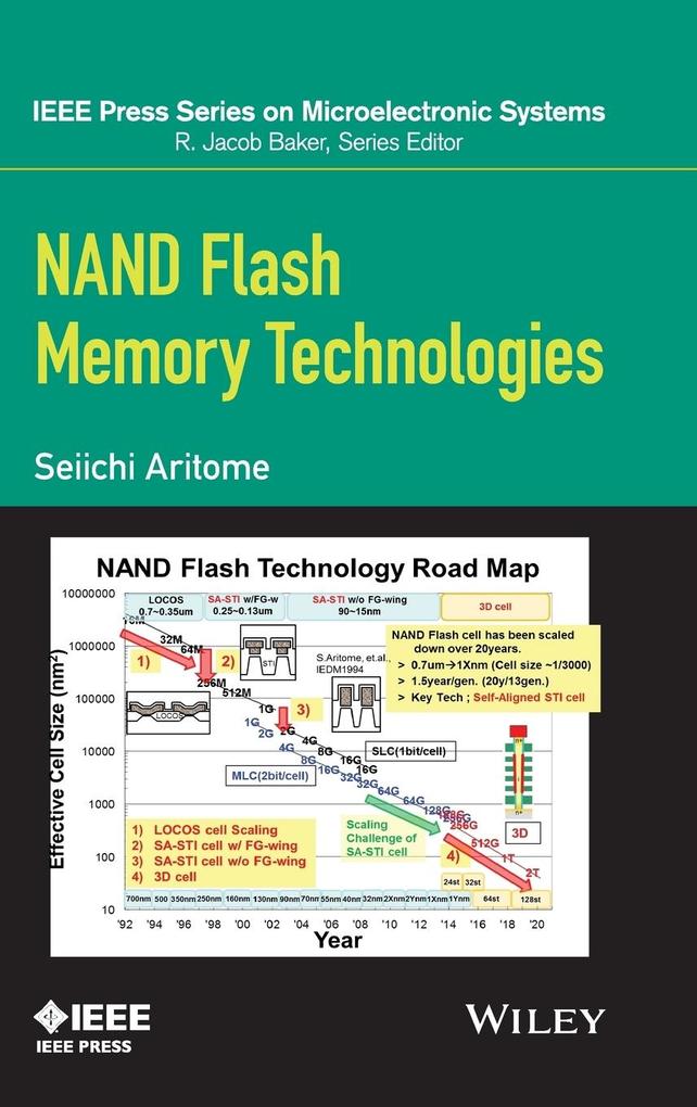
* Offers a comprehensive overview of NAND flash memories, with insights into NAND history, technology, challenges, evolutions, and perspectives
* Describes new program disturb issues, data retention, power consumption, and possible solutions for the challenges of 3D NAND flash memory
* Written by an authority in NAND flash memory technology, with over 25 years' experience
Inhaltsverzeichnis
Foreword xi Preface xv
Acknowledgments xvii
About the Author xix
1 Introduction 1
1. 1 Background, 1
1. 2 Overview, 8
References, 10
2 Principle of NAND Flash Memory 17
2. 1 NAND Flash Device and Architecture, 17
2. 1. 1 NAND Flash Memory Cell Architecture, 17
2. 1. 2 Peripheral Device, 19
2. 2 Cell Operation, 21
2. 2. 1 Read Operation, 21
2. 2. 2 Program and Erase Operation, 21
2. 2. 3 Program and Erase Dynamics, 28
2. 2. 4 Program Boosting Operation, 31
2. 3 Multilevel Cell (MLC), 34
2. 3. 1 Cell Vt Setting, 34
References, 35
3 NAND Flash Memory Devices 37
3. 1 Introduction, 37
3. 2 LOCOS Cell, 40
3. 2. 1 Conventional LOCOS Cell, 40
3. 2. 2 Advanced LOCOS Cell, 40
3. 2. 3 Isolation Technology, 43
3. 2. 4 Reliability, 46
3. 3 Self-Aligned STI Cell (SA-STI Cell) with FG Wing, 48
3. 3. 1 Structure of SA-STI Cell, 48
3. 3. 2 Fabrication Process Flow, 50
3. 3. 3 Characteristics of SA-STI with FG Wing Cell, 53
3. 3. 4 Characteristics of Peripheral Devices, 57
3. 4 Self-Aligned STI Cell (SA-STI Cell) without FG Wing, 59
3. 4. 1 SA-STI Cell Structure, 59
3. 4. 2 Fabrication Process, 60
3. 4. 3 Shallow Trench Isolation (STI), 61
3. 4. 4 SA-STI Cell Characteristics, 64
3. 5 Planar FG Cell, 66
3. 5. 1 Structure Advantages, 66
3. 5. 2 Electrical Characteristics, 68
3. 6 Sidewall Transfer Transistor Cell (SWATT Cell), 69
3. 6. 1 Concept of the SWATT Cell, 70
3. 6. 2 Fabrication Process, 71
3. 6. 3 Electrical Characteristics, 74
3. 7 Advanced NAND Flash Device Technologies, 77
3. 7. 1 Dummy Word Line, 77
3. 7. 2 The P-Type Floating Gate, 82
References, 89
4 Advanced Operation for Multilevel Cell 93
4. 1 Introduction, 93
4. 2 Program Operation for Tight Vt Distribution Width, 94
4. 2. 1 Cell Vt Setting, 94
4. 2. 2 Incremental Step Pulse Program (ISPP), 95
4. 2. 3 Bit-by-Bit Verify Operations, 98
4. 2. 4 Two-Step Verify Scheme, 99
4. 2. 5 Pseudo-Pass Scheme in Page Program, 102
4. 3 Page Program Sequence, 104
4. 3. 1 Original Page Program Scheme, 104
4. 3. 2 New Page Program Scheme (1), 107
4. 3. 3 New Page Program Scheme (2), 108
4. 3. 4 All-Bit-Line (ABL) Architecture, 111
4. 4 TLC (3 Bits/Cell), 113
4. 5 QLC (4 Bits/Cell), 115
4. 6 Three-Level (1. 5 Bits/Cell) NAND flash, 119
4. 7 Moving Read Algorithm, 122
References, 123
5 Scaling Challenge of NAND Flash Memory Cells 129
5. 1 Introduction, 129
5. 2 Read Window Margin (RWM), 130
5. 2. 1 Assumption for Read Window Margin (RWM), 131
5. 2. 2 Programmed Vt Distribution Width, 135
5. 2. 3 Vt Window, 137
5. 2. 4 Read Window Margin (RWM), 139
5. 2. 5 RWM Vt Setting Dependence, 140
5. 3 Floating-Gate Capacitive Coupling Interference, 142
5. 3. 1 Model of Floating-Gate Capacitive Coupling Interference, 142
5. 3. 2 Direct Coupling with Channel, 145
5. 3. 3 Coupling with Source/Drain, 148
5. 3. 4 Air Gap and Low-k Material, 149
5. 4 Program Electron Injection Spread, 153
5. 4. 1 Theory of Program Electron Injection Spread, 153
5. 4. 2 Effect of Lower Doping in FG, 158
5. 5 Random Telegraph Signal Noise (RTN), 161
5. 5. 1 RTN in Flash Memory Cells, 161
5. 5. 2 Scaling Trend of RTN, 166
5. 6 Cell Structure Challenge, 170
5. 7 High-Field Limitation, 171
5. 8 A Few Electron Phenomena, 175
5. 9 Patterning Limitation, 178
5. 10 Variation, 179
5. 11 Scaling impact on Data Retention, 183
5. 12 Summary, 185
References, 186
6 Reliability of NAND Flash Memory 195
6. 1 Introduction, 195
6. 2 Program/Erase Cycling Endurance and Data Retention, 198
6. 2. 1 Program and Erase Scheme, 198
6. 2. 2 Program and Erase Cycling Endurance, 200
6. 2. 3 Data Retention Characteristics, 203
6. 3 Analysis of Program/Erase Cycling Endurance and Data Retention, 210
6. 3. 1 Program/Erase Cycling Degradation, 210
6. 3. 2 SILC (Stress-Induced Leakage Current), 216
6. 3. 3 Data Retention in NAND Flash Product, 219
6. 3. 4 Distributed Cycling Test, 222
6. 4 Read Disturb, 224
6. 4. 1 Program/Erase Scheme Dependence, 224
6. 4. 2 Detrapping and SILC, 229
6. 4. 3 Read Disturb in NAND Flash Product, 234
6. 4. 4 Hot Carrier Injection Mechanism in Read Disturb, 235
6. 5 Program Disturb, 238
6. 5. 1 Model of Self-Boosting, 238
6. 5. 2 Hot Carrier Injection Mechanism, 244
6. 5. 3 Channel Coupling, 248
6. 6 Erratic Over-Program, 250
6. 7 Negative Vt shift phenomena, 253
6. 7. 1 Background and Experiment, 253
6. 7. 2 Negative Vt Shift, 254
6. 7. 3 Program Speed and Victim Cell Vt Dependence, 256
6. 7. 4 Carrier Separation in Programming Conditions, 260
6. 7. 5 Model, 262
6. 8 Summary, 263
References, 266
7 Three-Dimensional NAND Flash Cell 273
7. 1 Background of Three-Dimensional NAND Cells, 273
7. 2 BiCS (Bit Cost Scalable Technology) / P-BiCS (Pipe-Shape BiCS), 276
7. 2. 1 Concept of BiCS, 276
7. 2. 2 Fabrication Process of BiCS, 278
7. 2. 3 Electrical Characteristics, 279
7. 2. 4 Pipe-Shaped BiCS, 285
7. 3 TCAT (Terabit Cell Array Transistor)/V-NAND (Vertical-NAND), 289
7. 3. 1 Structure and Fabrication Process of TCAT, 289
7. 3. 2 Electrical Characteristics, 292
7. 3. 3 128-Gb MLC V-NAND Flash Memory, 294
7. 3. 4 128-Gb TLC V-NAND Flash Memory, 296
7. 4 SMArT (Stacked Memory Array Transistor), 298
7. 4. 1 Structural Advantage of SMArT, 298
7. 4. 2 Electrical Characteristics, 301
7. 5 VG-NAND (Vertical Gate NAND Cell), 302
7. 5. 1 Structure and Fabrication Process of VG-NAND, 302
7. 5. 2 Electrical Characteristics, 305
7. 6 Dual Control Gate-Surrounding Floating Gate Cell (DC-SF Cell), 308
7. 6. 1 Concern for Charge Trap 3D Cell, 308
7. 6. 2 DC-SF NAND Flash Cells, 309
7. 6. 3 Results and Discussions, 313
7. 6. 4 Scaling Capability, 317
7. 7 Advanced DC-SF Cell, 317
7. 7. 1 Improvement on DC-SF Cell, 317
7. 7. 2 MCGL Process, 319
7. 7. 3 New Read Scheme, 319
7. 7. 4 New Programming Scheme, 325
7. 7. 5 Reliability, 329
References, 329
8 Challenges of Three-Dimensional NAND Flash Memory 335
8. 1 Introduction, 335
8. 2 Comparison of 3D NAND Cells, 336
8. 3 Data Retention, 339
8. 3. 1 Quick Initial Charge Loss, 339
8. 3. 2 Temperature Dependence, 342
8. 4 Program Disturb, 343
8. 4. 1 New Program Disturb Modes, 343
8. 4. 2 Analysis of Program Disturb, 345
8. 5 Word-Line RC Delay, 350
8. 6 Cell Current Fluctuation, 353
8. 6. 1 Conduction Mechanism, 353
8. 6. 2 VG Dependence, 358
8. 6. 3 Random Telegraph Noise (RTN), 360
8. 6. 4 Back-Side Trap in Macaroni Channel, 363
8. 6. 5 Laser Thermal Anneal, 366
8. 7 Number of Stacked Cells, 368
8. 8 Peripheral Circuit Under Cell Array, 370
8. 9 Power Consumption, 371
8. 10 Future Trend of 3D NAND Flash Memory, 374
References, 376
9 Conclusions 381
9. 1 Discussions and Conclusions, 381
9. 2 Perspective, 384
References, 385
Index 389